


LioniX International is a vertically integrated supplier of custom photonic integrated circuit (PIC) solutions. We are an integrated photonics foundry, photonic chips design house, packaging provider, and IP developer, all rolled into one. Our proprietary technology is TriPleX® silicon nitride.
Photonic Integrated Circuits Solutions


Photonic Chips Custom Design & Packaging


Integrated Photonics Modules & Systems


 https://lionix.janlucas.nl/wp-content/uploads/2024/01/3301a-SatraX-Wafer-with-optical-beamer-network-devices.jpg
1365
2048
Ahmad Mohammad
https://lionix.janlucas.nl/wp-content/uploads/2017/01/Logo-Lionix-International.gif
Ahmad Mohammad2021-06-07 17:46:022025-12-10 17:18:49Markets
https://lionix.janlucas.nl/wp-content/uploads/2024/01/3301a-SatraX-Wafer-with-optical-beamer-network-devices.jpg
1365
2048
Ahmad Mohammad
https://lionix.janlucas.nl/wp-content/uploads/2017/01/Logo-Lionix-International.gif
Ahmad Mohammad2021-06-07 17:46:022025-12-10 17:18:49Markets


 https://lionix.janlucas.nl/wp-content/uploads/2026/02/4.png.webp
1080
1920
Lukas Janko
https://lionix.janlucas.nl/wp-content/uploads/2017/01/Logo-Lionix-International.gif
Lukas Janko2026-02-09 16:52:282026-02-12 11:05:52Global Photonics Engineering Contest 2026
https://lionix.janlucas.nl/wp-content/uploads/2026/02/4.png.webp
1080
1920
Lukas Janko
https://lionix.janlucas.nl/wp-content/uploads/2017/01/Logo-Lionix-International.gif
Lukas Janko2026-02-09 16:52:282026-02-12 11:05:52Global Photonics Engineering Contest 2026


Photonic Integrated Circuits at LioniX International
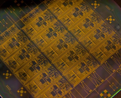
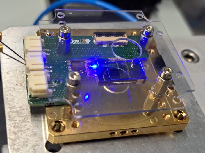
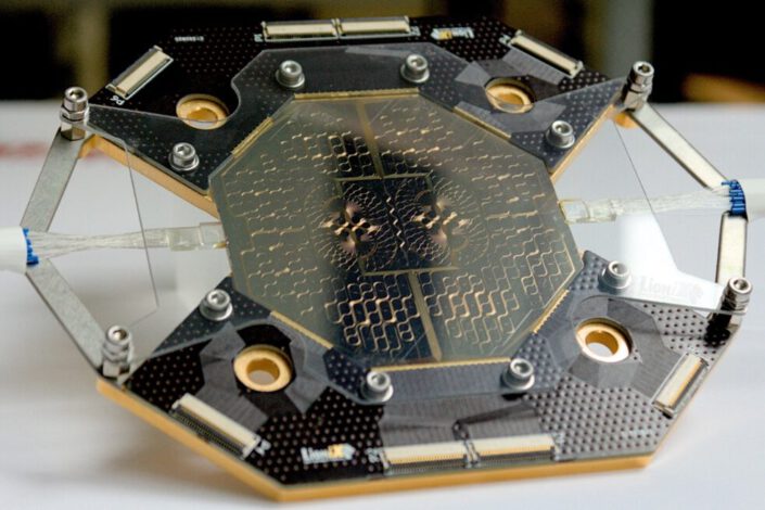
We fabricate silicon nitride photonic chips using our proprietary waveguide technology, TriPleX®. We also design integrated photonics circuits, assemble them with optical and electronic components, package them, and provide companion electronics to control them. We carry out all of these services in-house, and can work with custom and standard formats.
Our production volume capacity is flexible to support you during the whole product development cycle. We can provide demonstrators, single-unit prototypes, photonic chip pilot runs, and small to medium volume production, all in-house. For higher volume manufacturing, we are well-connected in the integrated photonics ecosystem and have vetted expert suppliers to work with. For lower volume experiments where a full wafer is not needed, we have low cost multi-project wafer shuttle runs, with reliable building blocks and a full-option PDK.
Our silicon nitride technology, TriPleX®, maintains ultra-low propagation and coupling losses. It is uniquely capable of integrating vertical and horizontal spot size converters (tapers). It allows for heat-based and stress-based modulation without any extra optical losses. It is transparent to wavelengths from 405 nm to 2350 nm, with a fully customizable layer stack.
Our integrated photonic chips and modules are used in a suite of high-tech applications in telecom and datacom, quantum, LiDAR, biosensors, AR and VR, and other markets. We are open to work with experts in any field: you know your market, and we know our photonics.
Learn more about integrated photonic chips
What are photonic integrated circuits?
Photonic integrated circuits (abbreviated to PIC or PICs) are semiconductor chips that work with light instead of electricity. They are the light-based counterpart to integrated circuits (ICs). Like ICs, PICs solve problems in innumerable fields, from computer processors to digital communication to precision sensing to automated device control to medical diagnostics.
PICs are sometimes called integrated photonics or integrated optics, which refers to the technical process by which optical systems are redesigned to fit into a chip. Optical systems rely on lenses, mirrors, and bulky electronic equipment to generate, manipulate, and detect light. These often involve optical benches, which are large, precisely manufactured tables where such optical components can be placed and moved around accurately.
Integrating such functions on chips on the scale of millimeters requires various cleanroom processing technologies, which are similar to the ones used in semiconductor manufacturing. Chemical vapor deposition, wet and dry etching, photolithography, sputtering, bonding, and many more are carried out in contaminant-free, sometimes human-free labs, to realize the devices.
How does a photonic integrated circuit work?
Photonic chips rely on total internal reflection to direct and manipulate light. Modern high speed internet uses optical fibers, which use the same physics principle. Optical fibers and photonic chips are both waveguides, because their function is to guide the direction of moving light. Light waveguides are made out of two layers, a core where the light travels freely, and a cladding which surrounds the core on all sides and reflects light. The core and the cladding work together to keep light moving only inside the waveguide.
The difference between the two technologies is that fiber optics use optical fibers as their waveguide, and integrated optics use silicon chips with waveguides built into them. Integrated waveguides are about a thousand times narrower than human hairs. Their reduced size makes integrated devices much smaller than fiber devices, and makes new designs and functions possible.
What problems do integrated photonics solve?
There are many applications where a photonic chip can outperform conventional electronic chips. Light can carry signals that are much more information-dense than electricity. Using photonic chips to process information is therefore faster and more energy efficient. For that reason, communication technologies were the first to commercialize the use of photonic integrated circuits. Light is also more sensitive to environmental changes, so photonic chips can be used as very sensitive sensors in biological applications and in quantum computing. Nothing travels faster than light, which means photonic chips can be used to make very fast distance measurements at very high accuracies. The range of applications in which photonic integrated circuits shine are only increasing more industries are exploring the possibilities of this technology.
Integrated photonics technology breakdowns from our PIC experts
Fabrication and Assembly of an AR/VR Light-Engine Prototype in Project MatEl
New Photonic Integrated Tuneable EC Laser with PZT Actuators
Reconfigurable (DE)MUX Filter for Flexible Frequency Allocation
Quantum scientists give Triplex® a HUG to entangle single photons
Want lower RF drift? Double down on laser PICs!